Applications
- Various Measuring Instruments
- LN Modulator
- Smart Glass
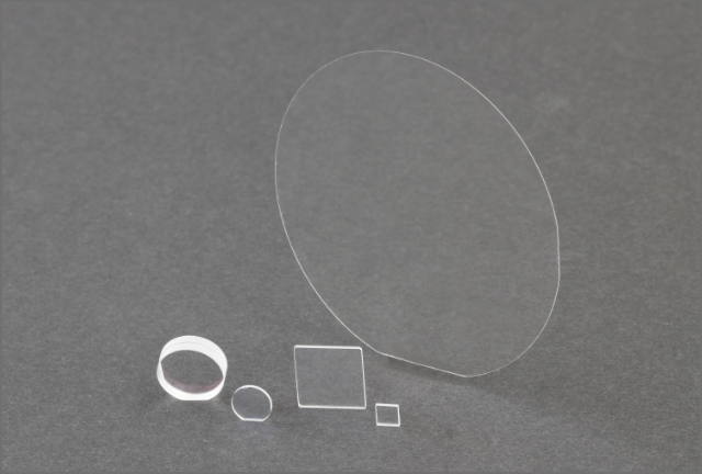
Features
- High quality quartz crystal wave plate with synthetic quartz crystals grown in-house used as the birefringent material.
- We can accommodate phase accuracy up to ± 1° with high-precision thickness processing accuracy.
- According to your requirements, we can design and supply any design wavelengths and/or retardations.
- We can offer multi, compound, and true zero order types.
- Large sizes and thin types are available.
- We can accommodate external dimensions up to 4 inches and thicknesses from 50 µm at minimum for true zero order.
We can also perform chipping from wafers upon request.
Retardance
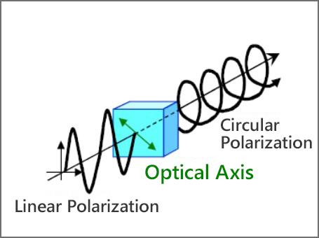
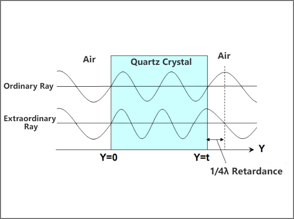
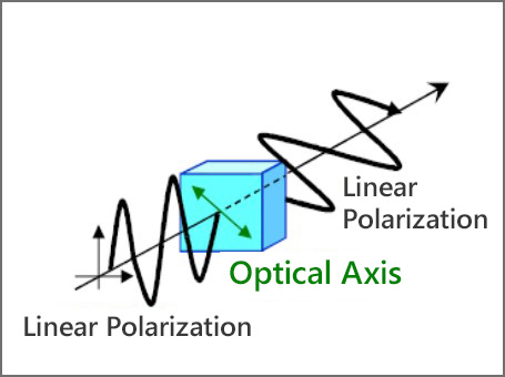
A λ/4 wave plate can convert linear polarization into circular polarization, while a λ/2 wave plate can convert into linear polarization with the plane of polarization rotated by 90°.
λ/4 Wave Plate
λ/2 Wave Plate

Standard Specifications
| Waveplate Type | Multiple Zero Order | Zero Order | True Zero Order |
|---|---|---|---|
| Material/Composition | Quartz/Single Plate | Quartz/2 layers | Quartz/Single Plate |
| Retardance | 1/4λ and 1/2λ | 1/4λ and 1/2λ | λ/2 λ/4 |
| Retardance Accuracy | ±λ/200(※1) | ±λ/200(※1) | ±λ/200(※1) |
| Design Wavelength[nm] | 266~1550 | 266~1550 | 1030~1550 |
| Sizes[mm] | Dia.152.4 Max. | Dia.76.2 Max. | Dia.76.2 Max. |
| Surface Quality | 20-10 | 20-10 | 20-10 |
| Coating Type R[%] Per Surface |
V Coat R<0.2% |
V Coat R<0.2% |
V Coat R<0.2% |
| Mount Frame Available | Yes | Yes | Yes |
| Remarks | Available Bonding method: Glue(acrylic) Optical Contact |
Thickness limitation 80μm Min.@Dia.76.2 mm 50μm Min.@Dia.25.4 mm |
*1 Consultation regarding phase tolerance may be required depending on the external size.
True Zero Order Wave Plate
λ/2 Wave Plate
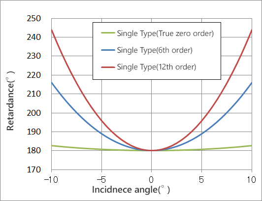
Relationship between Retardance and Incidnece Angle
λ/4 Wave Plate
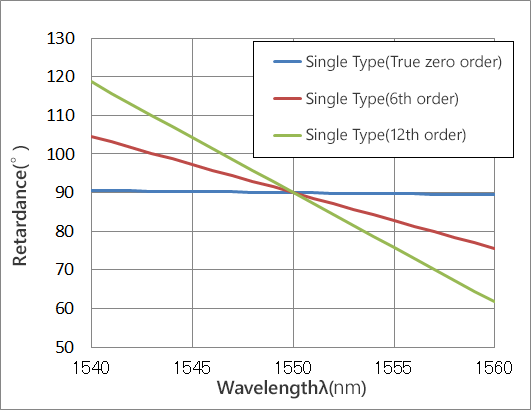
Relationship between Retardance and Wavelength
Product Lineup Example
- Circular plate and square plate are also available.
- Polish and rap surfaces are also available.
- Correspondence with a coat is also possible. Please provide the specificaitons.
| Material | Quartz Single Crystal |
|---|---|
| External Dimensons External Dimensional Tolerance |
Max.DIA.76mm(Available for chip size) ±0.1mm |
| Thickness | Min. 80μm |
| Retardation Retardance Accuracy |
λ/2 or λ/4 ±λ/200 |
| Transmitted Wavefront Accuracy | ~λ/4(@633nm) |
| Parallelism | <5arcsec |
| Surface Quality | 20-10 |
| Antireflection Coating | R≦0.2% per one side |
| Mount Frame Available | Yes |
Remarks)
- 1)The above shows the maximum size for available.
- 2)Quartz crystal has 573℃ transition temperature. Therefore, you shold use it at a temperature less than that.
*Please inquire for special specifications.
Warranty Items
Test items include temperature, humidity, impact resistance, heat resistance, etc. for the environmental and mechanical properties of optical components.
We set test items and conditions for each component and guarantee the properties of the component. However, warranty items and conditions vary depending on the shape, properties, application, and environment of the optical component.
| Subjected to High Temperature | 85℃ 1000H |
|---|---|
| Subjected to Low Temperature | -40℃ 1000H |
| Subjected to High Temperature and High Humidity | 60℃90%RH~95%RH 1000H |
| Heat Shock | -40℃ 2H 、85℃ 2H、100℃/H 10 Cycles |
| Subjected to Thermal Shock | -40℃/85℃ 30 Minutes Each 30 Cycles |
| Coating Adhesion Strength | Cellophane tape (LP-18) is applied to the component, rubbed with the fingers three times, and then quickly pulled off in a vertical direction ten times |
| Abrasion Resistance | The vapor-deposited surface is pressed with lens-cleaning paper (DUSPER K-3) with a pressing pressure of 4.9 N/cm2 (500 gf/cm2)
1 round-trip/second continuous, round-trip distance 10 mm, 100 round-trips |
| Solvent Resistance Test | Using lens-cleaning paper (DUSPEP K-3) in solvents such as IPA, acetone, ethanol, etc. with 2.94 N (300 gf) 1 round-trip/second continuous, round-trip distance 10 mm, 100 round-trips |
Optical Component

