NDK NIHON DEMPA KOGYO CO.,LTD.


Search within NDK


[PDF ]

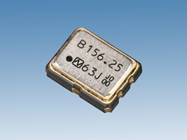
NP3225SBB (for Fixed Communication)

Features

  • Differential Output SPXO
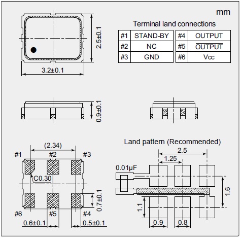
  • Compact dimension : 3.2×2.5×0.9mm.
  • Supply voltage : +2.5V or +3.3V.
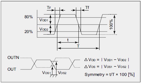
  • Output Specification : LVDS
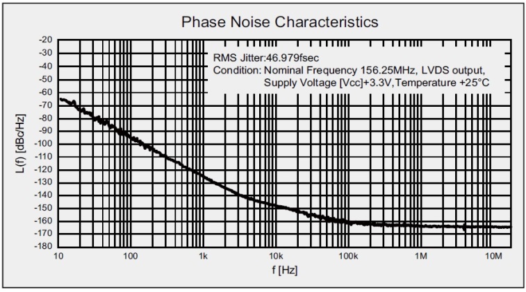
  • Excellent low phase jitter. (Typ. 47fs @156.25MHz)

NP3225SBB_picture

  • RoHS compliant
  • Pb Free
 

Specifications

Nominal Frequency Range (MHz) 100 to 170
Package Size (L×W×H : mm) 3.2×2.5×0.9
Output Specification LVDS
Overall Frequency Tolerance (*1) Max. ±50×10-6
Operating Temperature Range (°C) -40 to +85
Storage Temperature Range (°C) -55 to +125
Supply Voltage [VCC](V) +2.5±5 % +3.3±10 %
Current Consumption
(@ +25°C)
Enable (mA) Max. 40 (STAND-BY=VCC or OPEN, RL=100Ω)
Stand-by (µA) Max. 30 (STAND-BY=GND)
Output Voltage VOD1, VOD2 : +0.247 to +0.454V (Differential output voltage)
∆VOD : Max. 50mV (Differential output voltage)
VOS1, VOS2 : +1.125 to +1.375V (Differential output voltage)
∆VOS : Max. 50mV (Differential output voltage)
Rise Time / Fall Time (ns) Max. 0.4 (20 to 80% Waveform)
Symmetry (%) 45 to 55 (at 50% Waveform)
Output Load [RL] (Ω) 100 (Differential output voltage)
Start-up Time (ms) Max. 10
Phase Jitter (fs)
(@+3.3V, +25°C)
Typ. 47 (156.25MHz)
(Offset Frequency : 12kHz to 20MHz)
Specification Number NSC5187A NSC5187B

*1. The frequency stability includes initial frequency tolerance, temperature variation, and supply variation.

Please specify the model name, frequency, and specification number when you order products. For further questions regarding specifications, please feel free to contact us.

Dimensions

NP3225SBB Dimensions

Output Waveform

NP3225SBB Output Waveform

Phase Noise Specification


NP3225SBB Output Phase Noise Specification


Copyright© 1997- NIHON DEMPA KOGYO CO., LTD.