[PDF ]
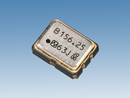
NP3225SBD (for Fixed Communication)
Features
- Differential Output SPXO
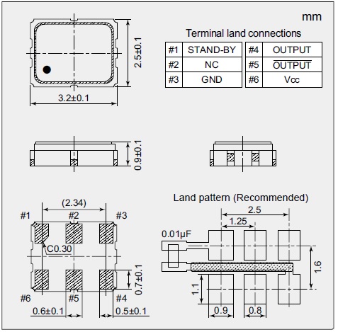
- Compact dimension : 3.2×2.5×0.9mm.
- Overall Frequency Tolerance Max. ±25×10–6 at –40 to +85°C.
- Supply voltage : +3.3V.
- Output Specification : LVDS
- Conforms to AEC-Q200.
Specifications
Dimensions
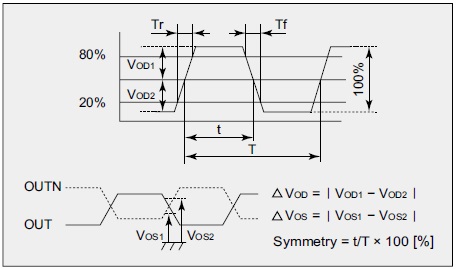
Output Waveform