![]()
Site Search
Please enter a keyword
- Crystal Unit
- Crystal Oscillator
- Frequency Synthesizer
- Signal Generator
- Millimeter-Wave Converter
- Synthetic Quartz Crystal
- Optical Component
- QCM Sensor
- Outgas Analysis System
- Ultrasound Probe (Transducer)
- SAW Devices (Manufactured by NDK SAW devices Co., Ltd.)
-
Space
-
Infrastructure / Industrial Equipment
-
Automotive
-
Mobile
-
AV / OA, Medical, Healthcare, Household Appliance
-
Search from Connectivity Standards
Product Search
Technology
Differential Outputs of Crystal Oscillators
[  PDF ]
PDF ]
1. Background
In recent years, high-speed transmission of sensor data has been required as represented by image data transmission, and "differential transmission" is generally used for high-speed transmission systems.
"Demand for differential output crystal oscillators (hereinafter, differential output oscillator is increasing even in crystal oscillators, which is the reference clock source for data transmission, as the speed increases.
For this reason, we would like to discuss the differential signal in this report."
2. Clock rate and signal level
Generally speaking, crystal oscillators are known for single-phase output with Clipped Sine wave and CMOS wave (square wave) output is typical.
Clipped Sine wave outputs are used well in RF circuits because they have a waveform similar to a square wave, and unwanted harmonics are suppressed. TCXO (Temperature Compensated Crystal Oscillator) is known as a product of Clipped Sine wave output.
Since the CMOS wave output is a signal output corresponding to the logical levels used for digital signal processing, it is good for transmitting digital signals and is used as a clock for CPUs, etc.
Following figure is an example of the clock rate and signal level, assuming that the edge rate is a constant (V/sec fixed) regardless of the voltage (Fig. 1).
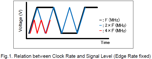
As shown in Fig.1, increasing the clock rate decreases the amplitude.
Minimizing the signal amplitude is important to accommodate high clock rates.
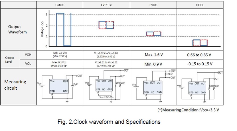
The CMOS output waveforms, output waveforms for small amplitude support, and specifications are shown below (Fig 2).
3. Characteristics of differential output waves
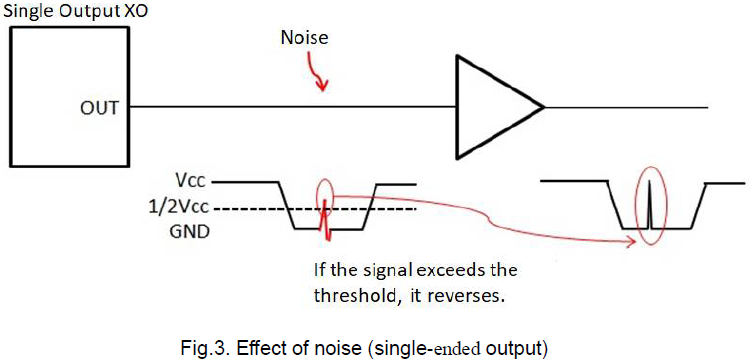
Small-amplitude waveform is susceptible to noises. For example, signal false recognition does not occur even if there is +1V noise in the CMOS waveform of the 3.3V (threshold +1.65V judgment), but if there is +1V GND noise in the CMOS waveform of +1.8V (threshold +0.9V judgment), the signal exceeds the threshold and invert, resulting false recognition.
Differential signals are effective as a means of preventing false recognition in this small-amplitude waveform.
Differential signals are characterized by the output of a reversed-phase waveform, each of which is inverted in phase, from a single-ended oscillator.
Since an opposite-phase signal is transmitted in one-to-one at equal amplitude and the difference is taken, it is less susceptible to external noise and GND.
The following image shows how the differential output XO can be canceled at the end of the output and received as a signal without noise even if it is affected by GND noise, and how the single-ended output oscillator is affected by noise (Fig. 4).
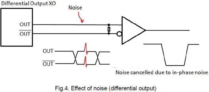
In this way, the influence of noise can be prevented by using a differential output.
4. Advantages and notes of differential signals
The advantages of differential signals are that when used terminated, there is no ringing in the waveform.
In contrast, since the single-ended output signal is not terminated, ringing is likely to occur, and harmonics are significantly observed, which may be disadvantageous to EMI, etc.
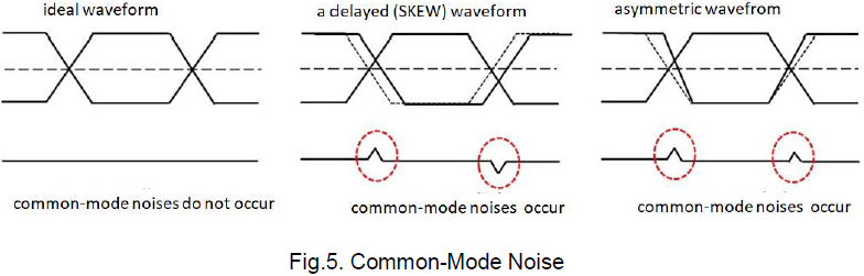
The symmetry of each signal waveform is critical for differential signal.
If there is a delay (SKEW) in one waveform, or if there is an asymmetric of the waveform, common-mode noise that affects signal quality such as EMI occurs (Fig. 5).
5. Advantages of differential output crystal oscillators
It is possible to generate a differential signal (waveform) by receiving waveform conversion on the system IC using a single output crystal oscillator.
However, because it is difficult to design a circuit that does not generate a delay (SKEW) between waveform, a signal with no delay (SKEW) can be obtained between waveform by a specially designed differential output crystal oscillator, thereby reducing the risk of system malfunction.
In high-speed DDR3 memories, the DDR (Double Data Rate) method is used to transmit data on the rising and falling edges of the clock.
However, it is difficult for the system IC side to acquire the waveform of the falling edges. In this field, the DDR function can be enabled by using the rising edges of the output signals of the differential output crystal oscillators.
NDK will continue to expand its lineup of differential output crystal oscillator that pursue the qualities of these waveforms to suit your application.