![]()
Site Search
Please enter a keyword
- Crystal Unit
- Crystal Oscillator
- Frequency Synthesizer
- Signal Generator
- Millimeter-Wave Converter
- Synthetic Quartz Crystal
- Optical Component
- QCM Sensor
- Outgas Analysis System
- Ultrasound Probe (Transducer)
- SAW Devices (Manufactured by NDK SAW devices Co., Ltd.)
-
Space
-
Infrastructure / Industrial Equipment
-
Automotive
-
Mobile
-
AV / OA, Medical, Healthcare, Household Appliance
-
Search from Connectivity Standards
Product Search

NDK photolithography technology adopted
in the latest 5G smartphones
NDK's crystal blank became first to receive
Qualcomm certification for IC due to superior temperature characteristics
NDK's crystal devices are playing a vital role in the expanding world of 5G communications. The advance in smartphone technology from LTE networks to 5G requiring high-frequency is expected to accelerate the adoption of NDK’s ultra-compact, high-frequency crystal devices.
Percentage of 5G devices in smartphone production
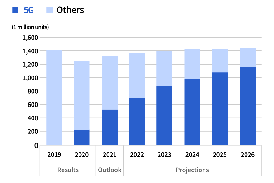
Fuji Chimera Research Institute, 2021 Worldwide Electronics Market Survey, March 2021
The shift to 5G mobile communications is increasing requirements for higher frequency clock sources and low phase noise in chipsets. A key challenge has been meeting carrier frequency band requirements, such as millimeter waves higher than 24 GHz. The frequency multiplication for internal clocks has increased, but higher multiplication produces more phase noise, creating concern that unstable signal phase and amplitudes could compromise reception sensitivity and reduce communication efficiency.
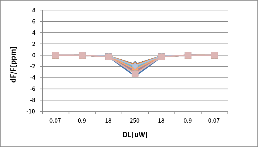
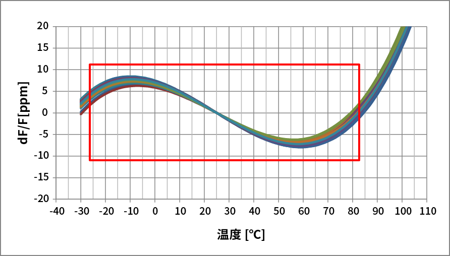
The proposed solution for improving phase noise was to reduce the frequency multiplication by raising the frequency from 38.4 MHz to 76.8 MHz for the internal reference oscillator source, and then to lower noise further by raising the crystal unit drive level to maintain stable temperature characteristic.
NDK met the challenge by advancing the crystal blanks it has been developing since 2008 to be more compact with higher frequency, and engineering them to accommodate photolithographic processing technology. Extensive trial and error led to an ideal external dimensions and configuration enabling compact, high-frequency, and high yield photolithographic blanks. The result of many years of intensive research is now ready to see the light of day.
Our photolithographic blanks provide excellent frequency stability at increased drive levels and exhibit highly stable characteristics with minimal frequency variation from temperature changes.
| DL vs ΔF/F | Temperature characteristics TC_F |
|---|---|
|
|
[Left: Drive level frequency stability, Right: Frequency temperature characteristics]
The superior characteristics of these photolithographic blanks fulfill the Qualcomm Technologies requirements for its 5G smartphone chipset* in the United States, making NDK its very first certified manufacturer of crystal devices.
Orders for the products have been growing steadily, and we are planning to expand our production lines to ensure a stable supply, with a target start of operation in July 2021.
* 5G Mobile Platform向けQualcomm Snapdragon 690, 750G
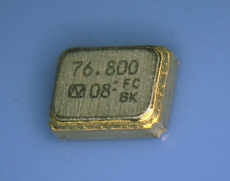
[The NX1612SD crystal unit
— the first ever to receive Qualcomm Technologies certification]
Advancing our cutting-edge photolithography technology
for the ongoing miniaturization of electronic devices
When we first began developing photolithographic blanks, we envisioned a future where electronic devices would become increasingly smaller, higher-performanced, and multifunctional. As electronic devices become smaller, we expect it to become increasingly difficult to process and manufacture crystal blanks for compact crystal devices with conventional mechanical methods. Photolithography technology provides a promising way forward.
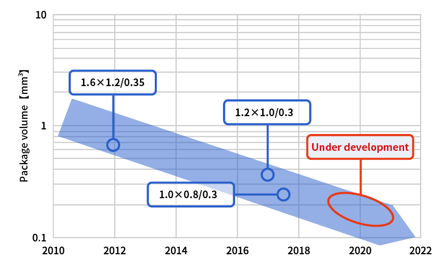
The miniaturization of crystal units
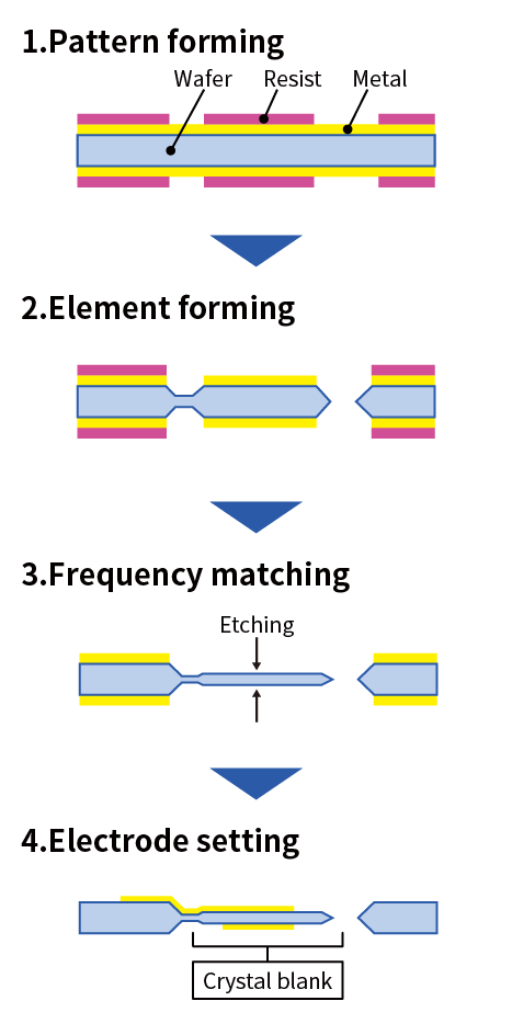
The production process of NDK for photolithographic blanks follows four steps. (1) A coating of metal and a resist layer mask are placed on a crystal substrate and pattern the mask for the external shape by exposing it to an electronic beam and development. (2) Wet etching then melts the crystal, leaving a pattern on the surface. (3) The resonance frequency, which is inversely proportional to the thickness of the base plate, is then set by using wet etching to attain the thickness for the desired frequency. (4) Electrodes are then set on the surface, completing the process.
NDK has refined this process leading to the mass production of compact, high-precision crystal blanks on the order of submicrons*. Our photolithographic blanks are used in 5G-compatible smartphones, True Wireless Stereo (TWS) earphones, and smartwatches, and are opening the way for devices that are increasingly smaller and thinner.
*Submicron: 1/10000mm
NDK photolithographic blank process flow (Outline drawing)
4-inch wafer
for stable mass production
Currently, the standard size of wafers for general photolithographic blanks is two inches. Only small wafers are able to be manufactured because it has been difficult to achieve stable frequency characteristics on larger wafers, resulting in a large quantity of unusable blanks being discarded.
However, NDK’s many years of research into large, high-quality raw crystals led to us becoming the first manufacturer to achieve mass production of 4-inch wafers, double the size of conventional wafers, with improved blank performance and an optimal yield of blanks per wafer. The increased blanks per wafer and the ability to stably-mass-produce crystal blanks with uniform quality reduce risk of wasting raw crystal and makes our process highly competitive in terms of both cost and quality.
NDK wafers offer superior raw crystal quality
NDK has the technology to grow and process raw quartz with very few crystal defects and that conforms to the 1aa grade IEC international standard.
![[Developing raw crystals]](../shared/images/under/photo/img_nuture.jpg)
[Developing raw crystals]
![[Large, high-quality raw crystals]](../shared/images/under/photo/img_crystal.jpg)
[Large, high-quality raw crystals]
![[Photolithographic process]](../shared/images/under/photo/img_wafer.jpg)
[Photolithographic process]
Making large wafers requires large, highly pure quartz crystals. NDK grows and manufactures its own high-quality raw crystals for photolithographic blanks. The raw crystal is cut and microfabricated to make precisely-sized wafers. This technical expertise accumulated over many years is the crucial foundation for integrated production of high-quality, high-performance crystal blanks.
We are strictly preserving product quality from the initial raw crystals through to the final products as we seek to further increase production yields and maintain our competitive advantage in the market.