![]()
![]()
Site Search
Please enter a keyword
- Crystal Unit
- Crystal Oscillator
- Frequency Synthesizer
- Signal Generator
- Millimeter-Wave Converter
- Synthetic Quartz Crystal
- Optical Component
- QCM Sensor
- Outgas Analysis System
- SAW Devices (Manufactured by NDK SAW devices Co., Ltd.)
-
Space
-
Infrastructure / Industrial Equipment
-
Automotive
-
Mobile
-
AV / OA, Medical, Healthcare, Household Appliance
-
Search from Connectivity Standards
Product Search
Oscillation Circuit Evaluation Methods
Points for Preventing Abnormal Oscillation When Designing Oscillator Circuits
| (*1) This series explains the specific examples (design, process, construction method, handling, etc.) in which the product function becomes impossible to maintain or becomes defective and the entire set becomes defective, as well as the reason why the product becomes defective. |
[  PDF ]
PDF ]
1. For stable oscillation
Crystal units, which are passive components, needs to optimize the oscillation ng conditions with the customer's circuits.
When designing an oscillator circuit, it is important to confirm in advance that the crystal unit is matched with the oscillator circuit.
Problems such as non-oscillation or frequency misalignment may occur if the matching is not appropriate. In particular, abnormal oscillation phenomenon may lead to unexpected problems in the market, etc.
Based on past trouble cases, we propose preventive measures for abnormal oscillation.
2. What is abnormal oscillation?
"When the crystal unit oscillates in modes other than normal oscillation modes, it is called abnormal oscillation.
Other than the normal oscillation mode, there is oscillation by coupling with the unwanted response(spurious), overtone oscillation, etc."
3. Abnormal oscillation due to coupling with spurious
The AT-cut crystal unit uses the thickness shear mode as the oscillation mode, but there are many other unwanted response (spurious) modes (flexure and face-shear etc.) (Fig. 1).
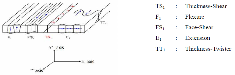
Fig. 1 Vibration mode of AT-CUT crystal unit
The higher order frequencies of these spurious may couple with the main vibration and affect the frequency temperature characteristics of the main vibration.
Equivalent circuit of the crystal unit including the unwanted response (spurious) is shown in Fig. 2.
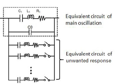
Fig. 2 Equivalent circuit of the crystal unit
Among the unwanted response (spurious) modes, there is a high risk of coupling to the main vibration, which is flexure and face-shear, and the frequency changes by changing the dimensions depending on the crystal element dimensions.
In addition, since the temperature characteristics of the main vibration and the flexure vibration are different, coupling with the main vibration occurs at a certain temperature when the temperature is changed, causing a phenomenon (Activity dip) in which the oscillation frequency changes rapidly, resulting in abnormal oscillation (Fig. 3).
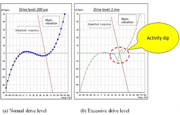
Fig. 3 Dependence of Activity dip on drive level (*2)
For this reason, NDK suppresses these unwanted response and prevents Activity dip by optimizing the crystal element and electrodes dimensions of the crystal unit.
However, note that if a drive level exceeding the crystal unit specifications is applied when designing the oscillation circuit, Activity dip may occur due to coupling of the main vibration with the unwanted response.
When measuring drive level, measure the crystal current (i) flowing into the crystal unit with a current probes and calculated from the crystal current (i), equivalent circuit constants of crystal unit(R1, C0), and load capacitance (CL) (*3).
| (*2) | drive level (DL): The power required for the crystal unit to oscillate. |
| (*3) | How to calculate drive level: DL=RL × i2 RL=R1(1+C0/CL)2 (RL=load resonance resistance, R1=resonance resistance, C0=shunt capacitance, CL=load capacitance) Please contact us separately for details of the measurement method of the crystal current (i). |
"When controlling the drive level during the oscillation circuit design, select an appropriate Rd (Fig. 4).
However, note that if the Rd-value is too large, the output level may be small, resulting in problems that the customer's subsequent circuits cannot be driven."
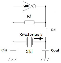
Fig.4 Oscillation Circuit and Crystal Current
4. Abnormal oscillation in crystal unit overtone mode
We have already stated that the AT-cut crystal unit uses the Thickness Slip mode, but the thickness of the crystal element and oscillation frequency can be calculated by the following formula:
F(MHz)=1.67 × n/t(mm) (n: overtone order, t: crystal element thickness)
For example, if the fundamental is 8 MHz, the third overtone is 24 MHz (Fig.5).
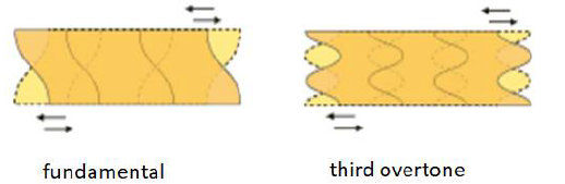
Fig.5 Thickness Shear Vibration
Fig. 6 shows the equivalent circuits of the crystal oscillators.
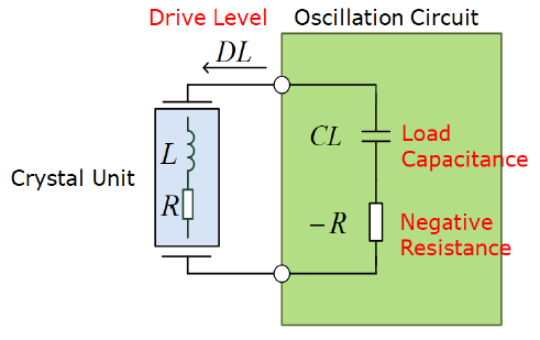
Fig. 6 Equivalent circuits of crystal oscillators
The oscillator circuit-side is indicated by a negative resistor (-R) and load capacitance (CL) and is not activated in the equivalent resistance below the crystal unit.
Whether to oscillate with the fundamental wave or with the third-order overtone is determined by the negative resistance characteristics (-R) of the IC, but the negative resistance of the oscillation circuit has frequency characteristics, that must be considered.
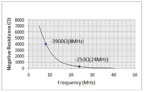
Fig.7. Frequency Characteristics of Negative Resistance
For example, when oscillating a crystal unit with a fundamental of 8 MHz only with a fundamental wave, the relationship shown in Fig. 7 lies in the negative resistance of the fundamental wave and the negative resistance of the third overtone.
Therefore, the negative resistance of the fundamental wave must be sufficiently ensured and oscillation must not occur in the third overtone.
If the typical value of the equivalent resistance is 120 Ω for the fundamental wave and 800 Ω for the third overtone at the SMD crystal unit of 8 MHz, oscillation is performed with the fundamental wave. In this case, there is no concern of oscillation with the third overtone.
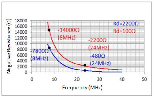
Fig.8 Frequency Characteristics of Negative Resistance (Effect of Rd)
However, as shown in Fig.8, if there is a negative resistance of -2200 Ω at 24 MHz as in the frequency characteristics of the negative resistance shown by the red line, oscillation of both the fundamental wave and the third overtone becomes possible.
Normally, the oscillation occurs with the fundamental wave that starts quickly at the start of oscillation. However, the oscillation may occur with the third overtone depending on the temperature environment, etc., which may cause abnormal oscillation.
In this way, when using an IC with large negative resistance in a wide frequency range, the negative resistance must be appropriately suppressed.
As a solution, add Rd in the oscillator circuit shown in Fig. 4 to control the current flowing into the crystal unit, and adjust the negative resistance.
Fig.8 blue line shows the negative resistance when Rd 2200 Ω is added. The negative resistance is -480 Ω for a third overtone equivalent resistance of 800 Ω, indicating that abnormal oscillations can be prevented.
5. To prevent abnormal oscillation
We have explained some examples of abnormal oscillation, but when designing oscillator circuits, we can prevent problems by thoroughly examining the matching between crystal unit and ICs.
"Please refer to NDK website for specific information on ICs and crystal unit matching.
If you can use the NDK's circuit analyses service at the prototype stage, we can propose an appropriate circuit constant."