![]()
![]()
Site Search
Please enter a keyword
- Crystal Unit
- Crystal Oscillator
- Frequency Synthesizer
- Signal Generator
- Millimeter-Wave Converter
- Synthetic Quartz Crystal
- Optical Component
- QCM Sensor
- Outgas Analysis System
- Ultrasound Probe (Transducer)
- SAW Devices (Manufactured by NDK SAW devices Co., Ltd.)
-
Space
-
Infrastructure / Industrial Equipment
-
Automotive
-
Mobile
-
AV / OA, Medical, Healthcare, Household Appliance
-
Search from Connectivity Standards
Product Search
Technology
Importance of Circuit Examination to Optimize Oscillation Circuit Configuration and Its Measuring Methods
(*1) This series explains the specific cases (design, process, construction method, handling, etc.) in which product performance cannot be maintained or the entire set becomes defective as a result of a product failure, as well as the reason why the product becomes defective.
[  PDF ]
PDF ]
When a crystal oscillator circuit is examined, troubles such as non-oscillation and frequency deviation can be prevented by investigating three items of [1] frequency, [2] negative resistance, and [3] drive level and verifying that the circuit is appropriate.
Nippon Dempa Kogyo Co., Ltd. (NDK) has implemented crystal unit in the customer's circuit board, checked the matching with crystal unit, and proposed appropriate conditions.
As a result of the circuit examination, more than seven percent of the cases have proposed any change, and as needed, we propose to change the specifications of crystal unit, change the IC used, change the circuit constants, and so on.
The measurement methods for the above three items are described below.
【1】 How do I correctly measure the frequency of the crystal oscillator circuit?
This section explains how to measure the oscillation frequency of the oscillation circuit.
1-1. Frequency measurement prone to trouble
A convenient method is to connect the measurement probe to the terminal of crystal unit. However, the frequency measurement value is negative with respect to the actual value and cannot be measured accurately.
This is because the input capacitance of a typical probe is around 13pF, and even a FET probe with a relatively small input capacitance is 2pF. Therefore, connecting the probe to crystal unit pin changes load capacitance CL.
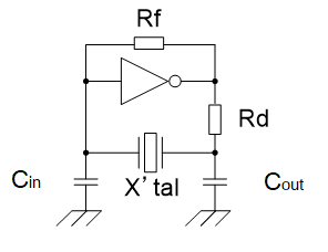
Fig. 1 Oscillation Circuit
For the oscillator shown in Fig. 1, load capacitance CL is shown in Equation 1.
CL=CinxCout / (Cin + Cout) + CS + CIC......(Equation 1) * CS: Floating capacitance of circuit CIC: Internal capacitance of IC
For example, if Cin=Cout=8pF, Cs=2pF, CIC= 4pF, CL is 10pF from Equation 1.
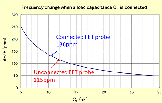
Fig. 2 Load capacitance characteristics
Fig. 2 shows an example of crystal unit showing the frequency change from nominal frequency(fnom) when a load capacitance CL is connected. The higher CL, the lower the frequency.
When the FET probe is not connected, the measurement oscillation frequency is +136ppm.
On the other hand, when the FET probes are connected, the 2pF load capacitance increases, resulting in getting +115ppm, 21 ppm lower than the actual value.
1-2. Non-contact Frequency Measurement Method Using Antenna
By measuring the crystal oscillation circuit without contact, the oscillation frequency can be accurately measured.
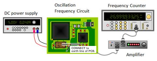
Fig.3 Non-contact Oscillation Frequency Measurement Method Using Antenna
Fig. 3 shows a case in which the antenna is placed close to crystal unit, the weak signals of the oscillator circuits are obtained without contacting, amplified by an amplifier, and measured by a frequency counter, etc. Since the antennas acquire frequencies on crystal unit without contacting them, they must be kept as close as possible.
In addition, connect the cable used for measurement to the PCB ground line.
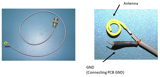
Fig. 4 Antenna
Fig. 4 shows an example of the antenna used by NDK, in which the end of the coaxial cable used for measurement is stripped and the core wire is coated. By creating a loop shape, the signal can be acquired efficiently.
1-3. Frequency Adjustment of Oscillator Circuit
By enabling non-contact frequency measurement, Cin, Cout values of Fig. 1 (oscillator circuits) can be changed to adjust the oscillation frequency to the actual purpose frequency, thereby increasing the accuracy of the oscillation frequency.
When crystal unit is shipped from NDK, the specified load capacitance is used to adjust the frequency.
If there is a large difference in frequency, load capacitance may be different. Please consult us.
【2】 How do We measure the negative resistance of a crystal oscillator circuit?
Many of the problems that occur in crystal unit do not oscillate when the power supply is turned on (non-oscillation).
To prevent non-oscillation, a sufficient negative resistor is required for the oscillator circuits, although it varies depending on the external dimensions and frequencies of crystal unit.
This section describes how to measure crystal unit start-up characteristics and negative resistance, which are important for designing oscillator circuits with appropriate negative resistance.
2-1. Crystal unit characteristics at start-up
When the power is turned on in the crystal oscillator, the natural frequency of crystal unit is selectively amplified from white noise and oscillation starts. Most crystal unit oscillation failures occur at startup (oscillation starts).
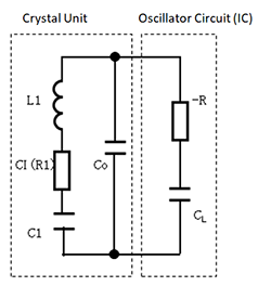
Fig.5 Equivalent Circuit of Oscillator Circuit
Fig. 5 shows the equivalent circuit of the oscillator circuit. An analysis was performed on the start of the oscillation circuit.
To obtain stable oscillations at startup, |-R|, which is the absolute value of the negative resistor (-R), must be sufficiently larger than load resonance resistance (RL) of crystal unit.
|-R|>RL....... (Equation 2)
By satisfying Equation 2, the oscillation grows and amplifies, and then becomes a steady state, resulting in a stable amplitude as shown in Fig. 6.
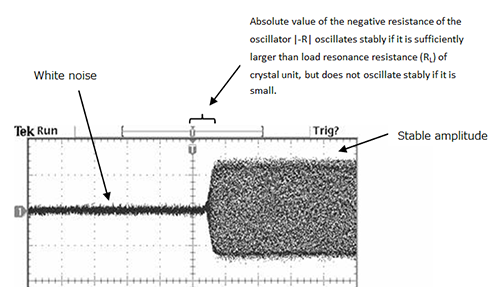
Fig. 6 Oscillation Circuit Characteristics at Start-up
2-2.Negative resistance tendency
The lower the frequency or the smaller crystal unit, the greater the required negative resistance. Negative resistance also varies depending on IC and frequency.
If the negative resistance is excessively large, problems such as 3rd overtone vibration mode or self-oscillation may occur.
2-3.Measuring method of negative resistance
Negative resistance can be measured by connecting a resistor to crystal unit and measuring the resistance that causes non-oscillation. In the same way as frequency measurement, the antennas are used to make measurements without being affected by stray capacitance by making the antennas contactless with crystal unit.
The resistance is initially set to a large value, and the resistance is gradually reduced from the state in which oscillation became non-oscillating.. The resistance value at the time when oscillation started is measured and this is regarded as a negative resistance. On the other hand, note that the value of the resistor that becomes non-oscillating by increasing the resistance value from the oscillating state is larger than the actual negative resistance value.
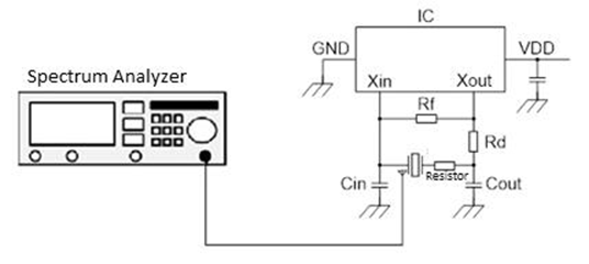
Fig. 7 Measuring method of negative resistance
【3】 How to measure drive level of a crystal oscillator.
This section explains how to measure drive level of crystal unit.
3-1. How to measure drive level
Measure the current Ip-p (mA) that flows through crystal unit with the current probe using an oscilloscope (Fig. 8).
Calculate the rms current Irms using Equation 3. From here, measure drive level using Equation 4.
Irms=Ip-p/(2√2) (mA)..... (Equation 3)
P=(Irms) 2 x RL(μW)...... (Equation 4)
※ RL=R1(1+Co/CL)2
Please inquire about shunt capacitance Co ,load capacitance CL, and R1 of crystal unit (Equation 4).
If the actually measured drive level is greater than the max. Drive level specified in the delivery specifications, it can be corrected by increasing the Rd of the oscillator in Fig. 1 and reducing the current flowing through crystal unit.
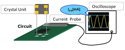
Fig. 8 Drive Level Measuring Diagram
3-2. Activity dip occurs if drive level is excessively high
If drive level applied to crystal unit is excessively high, the suppressed spurious may be excited, causing an activity dip in frequency/temperature characteristics. Therefore, use drive level below the values specified in the document of specifications.
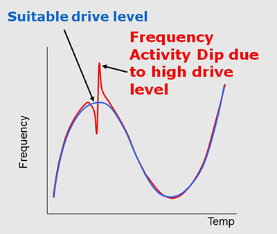
Fig. 9 Activity dip occurs when drive level is excessive
【Final】
Examining the circuit before using crystal unit and verifying that there are no problems with oscillation frequencies, negative resistances, drive level, etc., enables the user to optimize the circuit configuration of the oscillator circuit at board and eliminate problems. NDK offers a circuit examination service, so please be sure to consult with us.