![]()
Site Search
Please enter a keyword
- Crystal Unit
- Crystal Oscillator
- Frequency Synthesizer
- Signal Generator
- Millimeter-Wave Converter
- Synthetic Quartz Crystal
- Optical Component
- QCM Sensor
- Outgas Analysis System
- Ultrasound Probe (Transducer)
- SAW Devices (Manufactured by NDK SAW devices Co., Ltd.)
-
Space
-
Infrastructure / Industrial Equipment
-
Automotive
-
Mobile
-
AV / OA, Medical, Healthcare, Household Appliance
-
Search from Connectivity Standards
Product Search
Crystal Oscillator SPXO
NP2520SB
![]()
![]()
Application
・5G compatible equipment
・Optical communication, optical transceivers
・WDM equipment
Features
・LVDS Differential output SPXO
・Compact : 2.5 x 2.0 x 0.8 mm
・Supply voltage : +2.5V or +3.3V
・Low phase jitter:Typ. 100 fs @156.25 MHz
・Lead-free


| Item | Symbol | Value | Unit | ||
|---|---|---|---|---|---|
| Nominal frequency range | fnom |
|
MHz | ||
| Package size (L×W×H) | - | 2.5×2.0×0.8 | mm | ||
| Supply voltage | Vcc |
|
V | ||
| Current consumption | ICC |
|
mA | ||
| Stand-by current | IST |
|
μA | ||
| Output specification | - |
LVDS |
- | ||
| Load | RL | Typ. 100 | Ω | ||
| Storage temperature range | Tstr | -55 to +125 | ℃ | ||
| Operating temperature range | Topr |
|
℃ | ||
| Overall frequency tolerance *1 | Δf/fnom |
|
ppm | ||
| Output voltage | VOD |
|
V | ||
| Output voltage | ΔVOD |
|
mV | ||
| Output voltage | VOS |
|
V | ||
| Output voltage | ΔVOS |
|
mV | ||
| Rise (tr), fall (tf) time (20% to 80% WaveForm) | tr/tf |
|
ns | ||
| Symmetry (at 50 % Waveform) | SYM | 45 to 55 | % | ||
| Start-up time | tsu |
|
ms | ||
| Phase jitter (F = 156.25MHz) | tpj |
|
fs | ||
| Specification number | - |
|
- |
*1. The frequency stability Include Initial frequency tolerance, temperature variation, and supply variation.
Stand-by function
| #1 PAD input | #4, 5 PAD output |
|---|---|
| H Level (0.7 VCC to VCC) or OPEN | Operating |
| L Level (0.3 VCC max) | High impedance |
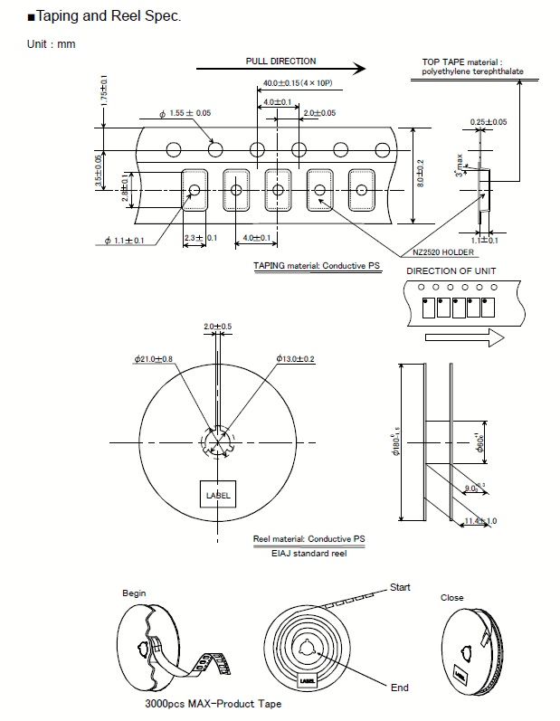
External dimensions

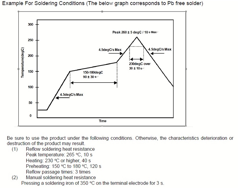
Output Wave 1
